Learn everything about PCB (Printed Circuit Board) manufacturing.
From design rules, materials, fabrication processes and assembly (SMT/through-hole), to testing and quality — with a practical UK manufacturing perspective featuring Roscan Electronics, a long-established contract electronics manufacturer. Keywords: PCB manufacturing, printed circuit board, PCB assembly, Roscan Electronics, UK PCB manufacturer, PCB prototype, HDI, SMT, rigid-flex.
Printed Circuit Boards (PCBs) are the physical backbone of nearly every electronic device — from consumer gadgets and medical instruments to industrial controllers and automotive electronics. This comprehensive guide explains how PCBs are designed, fabricated, assembled, and tested, and highlights what to look for when choosing a manufacturing partner. Throughout the article we’ll reference Roscan Electronics — a UK contract electronics manufacturer with long experience in PCB manufacturing and assembly — to show practical, real-world capabilities and considerations when moving a design from prototype to production.
Table of contents
- What is a PCB and why it matters
- Key PCB types and materials
- The PCB design → manufacturing lifecycle
- Step-by-step PCB fabrication processes
- PCB assembly: SMT, through-hole and hybrid approaches
- Testing, inspection and quality control (including IPC and ISO)
- Advanced and emerging PCB technologies (HDI, rigid-flex, embedded passives)
- Choosing a PCB manufacturing partner — what to ask Roscan (and other vendors)
- Cost drivers and ways to optimise for price and reliability
- Sustainability, RoHS, REACH and environmental considerations
- Detailed FAQ
1. What is a PCB and why it matters
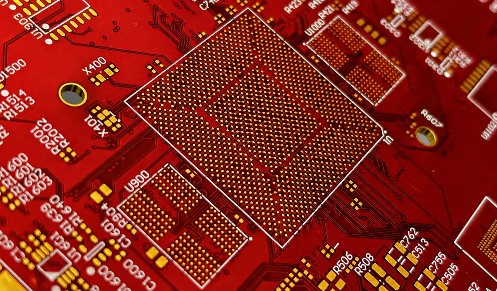
A Printed Circuit Board (PCB) mechanically supports and electrically connects electronic components using conductive tracks, pads, and other features etched from copper laminated onto a non-conductive substrate. PCBs replace point-to-point wiring with compact, repeatable layouts that enable modern miniaturised electronics, reliable mass production, and complex multi-layer designs. Because the PCB carries power, signals and often mechanical loads, its quality directly affects device reliability, signal integrity and manufacturability — so choosing the right board materials, layer stackup and fabricator early matters.
2. Key PCB types and materials
PCBs come in many flavors — each suited to different use cases:
- Single-sided PCBs — one copper layer; cheapest; used in simple electronics and cost-sensitive designs.
- Double-sided PCBs — copper on two sides, with plated through-holes to connect layers; common for moderate complexity.
- Multilayer PCBs — three or more copper layers laminated together with internal planes for power and signal routing; essential for high-density and high-speed designs.
- Rigid PCBs — the classic FR-4 (epoxy glass) board used in most consumer and industrial electronics.
- Flexible (flex) PCBs — polyimide or similar substrates that bend; used where space or mechanical movement requires flexibility.
- Rigid-flex PCBs — a hybrid that combines rigid boards and flexible sections; common in aerospace, medical devices and compact equipment.
- High-frequency/Low-loss materials — specialised laminates (e.g., Rogers) for RF, microwave, and high-speed digital applications.
Materials & stackups: FR-4 is the default for most applications; choices around Tg (glass transition temperature), copper weight (oz/ft²), dielectric thickness, and core/prepreg materials drive electrical performance and thermal robustness.
3. The PCB design → manufacturing lifecycle
A successful PCB project moves through these stages:
- Concept & schematic capture — define circuits, netlist and functional requirements.
- PCB layout & DFM — place parts, route signals, define layer stackup and design for manufacturability (DFM). DFM reduces avoidable fabrication and assembly issues later.
- Prototype — quick-turn prototype boards to validate form, fit and function.
- Pilot run — a limited production run to verify yield and assembly processes.
- Volume production — high-volume fabrication and assembly with mature, repeatable processes.
- Support & lifecycle — change control, obsolescence management and long-term sourcing.
Working with a manufacturer early — especially one that offers PCB fabrication and full product build services — speeds the transition between these stages and avoids costly redesigns. Roscan provides end-to-end services from board sourcing to full product build and electromechanical assembly, which is particularly helpful for companies that want a single supplier for prototype through production.
4. Step-by-step PCB fabrication processes
PCB fabrication turns the board design into a physical product. Key fabrication steps:
a) Artwork and data preparation
Gerber files (or ODB++) plus drill files and fabrication notes are prepared. Accurate layer naming, aperture lists and clear fabrication notes (e.g., controlled impedance requirements) speed quotes and reduce errors.
b) Inner layer imaging and etching (for multilayer boards)
Copper is laminated to cores; images are transferred using photolithography; unwanted copper is etched away to leave traces.
c) Lamination (multilayer)
Cores and prepreg are stacked and pressed under heat and pressure to form the multilayer board with reliable bonds; the chosen stackup determines controlled impedance and signal integrity.
d) Drilling & via formation
Precision drilling (mechanical or laser) creates through-holes, microvias or vias-in-pad for HDI boards. For blind/buried vias, sequential lamination or microvia drilling is used.
e) Plating
Through-holes and vias are plated with copper to establish reliable interlayer connections. Surface finish options (HASL, ENIG, OSP, immersion silver) are applied depending on assembly needs.
f) Soldermask & legend printing
Soldermask (green, black, white, etc.) is applied to insulate traces and prevent bridging, and legends/silk are printed for component reference.
g) Surface finish & routing
Final surface treatment and routing or v-scoring separates boards from the panel. Electrical test (flying probe or bed-of-nails) verifies continuity and isolation.
(SEO keywords: PCB fabrication steps, how PCBs are made, PCB etching, multilayer lamination, PCB surface finish)
5. PCB assembly: SMT, through-hole and hybrid approaches
PCB assembly populates bare boards with components. Main assembly methods:
Surface Mount Technology (SMT)
SMT is the default for modern electronics. Process flow:
- Stencil printing: solder paste applied to pads through a stainless-steel stencil.
- Pick & place: robotic machines place SMD components to tight tolerances (±0.05 mm or better).
- Reflow soldering: controlled oven profile melts solder paste to form reliable joints.
- Inspection: automated optical inspection (AOI) checks placement and solder quality.
Through-hole & wave soldering
Used for large or mechanically stressed components; through-holes may be manually inserted or wave-soldered. Through-hole provides mechanical strength.
Selective soldering
For mixed SMT/through-hole boards, selective soldering is used to avoid damaging SMT components with wave solder.
Conformal coating, potting and box-build
For environmental protection or ruggedisation, conformal coats or potting compounds are applied. Box-build integrates PCB assemblies into enclosures, adds cabling and final system testing — services offered by full contract manufacturers. Roscan provides PCB population, cable harness manufacture and electromechanical assembly at their UK facility.
6. Testing, inspection and quality control
Quality control ensures reliability and conformance:
- Incoming inspection: components and materials are checked against purchase specs and lot traces.
- In-process inspection: AOI after placement, wave or reflow inspection, visual checks.
- Electrical testing: flying probe tests (for prototypes and small runs) or bed-of-nails ICT fixtures (for volume production) validate continuity, shorts and basic functional blocks.
- Functional testing: simulated operational tests (power-up, firmware loading, I/O checks) to confirm device behaviour.
- X-ray inspection: used to inspect hidden solder joints (e.g., BGA underside).
- Standards and certifications: IPC standards (IPC-A-610 for acceptability) and ISO certifications (e.g., ISO 9001) are industry benchmarks.
Choosing a contract manufacturer with trained IPC engineers and ISO-certified processes reduces risk. Roscan highlights IPC-trained engineers and ISO 9001 accreditation, reflecting formal quality systems that many OEMs require.
7. Advanced and emerging PCB technologies
The electronics industry keeps pushing density, speed and integration. Key trends:
- High-Density Interconnect (HDI): microvias and finer traces enable denser routing and smaller packages (BGA, CSP). Roscan notes expertise in HDI PCBs for advanced electronics.
- Embedded components & passive integration: resistors/capacitors embedded within the substrate reduce board space.
- Additive PCB printing: emerging techniques print conductive inks for rapid prototyping and special applications.
- Flexible and rigid-flex designs: critical where space and motion are constrained (wearables, medical implants, aerospace).
- AI & Industry 4.0 in manufacturing: smarter pick-and-place, vision inspection and predictive maintenance increase yield and lower costs; Roscan publishes forward-looking articles on the future of PCB manufacturing and digitalisation.
8. Choosing a PCB manufacturing partner — what to ask Roscan (and other vendors)
When evaluating a fabricator / contract manufacturer, consider technical capability, quality systems, communication and supply chain resilience. Core questions:
- What PCB technologies do you support? (single/double/multilayer, rigid, flex, rigid-flex, HDI, controlled impedance). Roscan can source many board technologies from approved fabricators and supports rigid, flex and rigid-flex requirements.
- Can you do end-to-end services? (board sourcing, population, cable/harness, box-build, test). Roscan offers board population, cable harness manufacture and full electromechanical product build in the UK.
- What quality certifications and traceability do you provide? Look for ISO 9001, IPC training, RoHS/REACH compliance, and counterfeit-component policies. Roscan provides ISO 9001 certification and public policy downloads for RoHS and counterfeit avoidance.
- Are prototypes quick-turn? Rapid prototyping shortens iterations. Verify typical lead times and whether they have quick-turn services.
- How are obsolescence and long-term supply handled? For products with long lifecycles, supplier stability and component sourcing strategies matter.
- Where are boards sourced? Onshore vs offshore sourcing balances cost, lead time and IP risk. Roscan sources PCBs from approved fabricators both in the UK and offshore to balance capabilities and pricing.
9. Cost drivers and ways to optimise
Understanding cost drivers helps you make tradeoffs:
Cost drivers: number of layers, board size, copper weight, special materials (high Tg, Rogers), controlled impedance, via types (blind/buried), surface finish, panelisation and tolerances, low volume vs high volume runs, and component mix (BGAs and oddball parts increase assembly complexity).
Ways to optimise:
- Simplify layer count where possible and combine functions in fewer layers.
- Standardise board dimensions to fit efficient panel sizes and reduce waste.
- Avoid unnecessary tight tolerances if not required.
- Design for assembly (DFA): orient parts for easier placement, reduce manual insertion, and use standard footprints.
- Use common components to benefit from bulk pricing and simpler sourcing.
- Work with your manufacturer early to incorporate DFM suggestions — fabricators like Roscan can advise on achievable tolerances and more cost-efficient finishes.
10. Sustainability, RoHS, REACH and environmental considerations
Environmental and regulatory compliance is a growing factor for OEMs:
- RoHS (Restriction of Hazardous Substances): restricts lead, mercury, cadmium and other substances in electronics sold in many markets.
- REACH: EU regulation for chemicals; manufacturers typically publish REACH policy statements.
- Recyclability & materials: some substrates are more recyclable than others; designing for disassembly helps end-of-life recycling.
- Energy & waste: choosing manufacturers with environmental management systems (ISO 14001) and waste reduction programmes reduces the product’s lifecycle footprint.
Roscan publishes environmental and policy statements and provides documentation (RoHS, REACH) and certificates to assist customers in compliance and procurement.
11. Why work with a UK contract electronics manufacturer like Roscan?
There are strategic advantages to working with a UK-based contract electronics manufacturer:
- Proximity & communication: easier visits, technical collaboration and faster feedback loops.
- IP protection & security: onshore partners can be preferable for sensitive designs.
- Regulatory & procurement alignment: UK/EU regulatory understanding and ready documentation (ISO certificates, RoHS/REACH compliance) simplify audits.
- End-to-end services: companies like Roscan offer board sourcing, assembly (SMT & through-hole), cable & harness manufacture and box-build, providing a single accountable supplier for product builds. Roscan’s long history since 1977 and established facility in Wokingham/Finchampstead reflect decades of experience in contract electronics manufacturing.
Practical checklist: moving your PCB project to production
Use this checklist when you’re ready to engage a manufacturer:
- Finalise schematic and BOM with approved part alternatives (avoid single-source unless necessary).
- Produce clean fabrication data: Gerbers, drill files, assembly drawings, pick-and-place files, and stencil files.
- Define acceptance criteria: IPC class (1, 2 or 3), functional test procedures and burn-in requirements.
- Request quick-turn prototypes to validate mechanical fit and basic function.
- Run pilot production with full electrical/functional testing.
- Confirm documentation & certificates: ISO, RoHS, REACH, counterfeit component policy, traceability.
- Agree on change control and support plans for long-term production.
Roscan provides downloads of certificates, capability sheets and policies to assist customers in meeting procurement and audit requirements.
Case study snapshot (how a manufacturer like Roscan helps)
A common customer journey: a small UK OEM designs a control board for an industrial sensor. They need quick prototypes, assembly of low volumes (SMT + through-hole), cable harnesses and final box-build. By partnering with a full-service contract manufacturer, the OEM:
- Gets faster turnaround on prototypes (short feedback cycles).
- Reduces supplier management overhead — single point of accountability for boards, population and test.
- Gains access to manufacturing advice to optimise yield and reduce costs.
Roscan advertises exactly these services: PCB sourcing and manufacture, PCB population, cable harness manufacture and full electromechanical product build from their specialised Wokingham facility.
Final thoughts
PCB manufacturing is both a mature discipline and a field of rapid innovation. Whether you’re building a consumer device, medical instrument, or industrial controller, success depends on strong design practices, early collaboration with your fabricator/assembler, and robust testing & supply chain planning. Working with experienced, certified contract manufacturers — like Roscan Electronics in the UK, which combines long experience, ISO-level quality systems and a full suite of assembly and box-build services — can dramatically reduce risk and time-to-market.
FAQ — Printed Circuit Board (PCB) Manufacturing
Q1: What should my Gerber files include to avoid fabrication delays?
A: Provide industry-standard Gerber (RS-274X) files for each copper layer, soldermask, solder paste, and legend (silkscreen). Include a drill file (Excellon), a board outline, mechanical drawings (DXF/PDF) with dimensions and any special fabrication notes (controlled impedance targets, material requirements, blind/buried vias, via-in-pad, thickness). Also supply pick-and-place files and a centroid file for assembly. Clear layer naming, a README with netlist references and part orientation notes helps the fabricator cross-check data and speeds quoting and manufacture.
Q2: What PCB surface finish should I choose?
A: Common finishes: HASL (lead-free), ENIG (Electroless Nickel Immersion Gold), OSP (Organic Solderability Preservative), immersion silver and immersion tin. ENIG gives a flat, solderable surface good for BGAs and multiple reflows but costs more; HASL is economical but less planar; OSP is cheap and works for certain SMT processes but offers limited shelf life. Choose based on component types (e.g., BGA prefers planar ENIG) and expected handling/reflow cycles.
Q3: What is the difference between flying probe and ICT testing?
A: Flying probe uses moving probes to test nets and shorts without a fixed fixture; it’s flexible and ideal for prototypes/small runs. In-Circuit Testing (ICT) uses a bed-of-nails fixture to contact many nodes simultaneously, providing faster, high-coverage testing for volume production but requires a dedicated fixture (higher upfront cost). Choose flying probe for low volumes and ICT for high volumes where per-unit test time matters.
Q4: How long does PCB manufacturing and assembly take?
A: Lead times vary by complexity and volume. Quick-turn prototypes can be delivered in days to weeks; complex multilayer HDI boards or long lead components extend lead times. Assembly adds time for stencil making, component sourcing, pick-and-place and test. Work with your contract manufacturer to get realistic timelines — Roscan advertises both quick-turn and production services and can source boards from approved fabricators nearshore/offshore depending on need.
Q5: What are HDI PCBs and when should I use them?
A: HDI (High-Density Interconnect) PCBs use microvias, fine line widths and dense routing to achieve smaller form factors and more routing density — essential for smartphones, wearables, and compact medical devices. Use HDI when you need to place BGAs, reduce board size, or meet high routing density demands. Fabrication and assembly costs increase, so weigh performance vs cost.
Q6: How do I manage component obsolescence and supply chain risk?
A: Keep multiple approved alternate parts, maintain component lead-time monitoring, and work with manufacturers who provide sourcing support and last-time buy services. Consider stocking critical components or negotiating longer supply windows with vendors. Contract manufacturers with mature procurement teams can often mitigate shortages by leveraging supplier relationships.
Q7: What certifications and policies should a reputable contract manufacturer provide?
A: Look for ISO 9001 (quality management), IPC training/standards compliance, RoHS/REACH policy statements, counterfeit component policies, and documented quality and environmental policies. Roscan lists ISO 9001, policy downloads and capability brochures on their site, which help OEMs meet procurement and audit requirements.
Q8: Can a manufacturer do full product builds (box-build)?
A: Yes — many contract electronics manufacturers provide box-build services that combine PCB assembly, cable & harness manufacture, mechanical assembly, wiring, enclosure integration and final functional testing. This single-supplier model simplifies logistics and accountability. Roscan advertises electromechanical assembly and cable harness manufacture alongside PCB assembly.
Q9: How do I design for testability (DFT)?
A: Provide test points for access to critical nets, avoid burying testable nodes under components when possible, and design test fixtures into the board outline (e.g., pogo-pin locations). Plan for boundary-scan (JTAG) where applicable for digital device testing, especially for BGAs where bed-of-nails access is limited.
Q10: Is it better to source PCBs domestically or offshore?
A: It depends. Domestic sourcing (onshore) offers faster communication, potentially better IP protection, and lower logistics complexity; offshore sourcing often gives cost advantages for large volumes. Hybrid strategies — sourcing critical or complex boards domestically and volume boards offshore — provide a balance. Roscan sources PCBs from approved fabricators both in the UK and offshore to combine capability and cost considerations.
Roscan Electronics can be contacted at www.roscan.co.uk
Discuss your PCB Assembly & EMS requirements with our team
Contact Roscan Electronics
01189 737 287
sales@roscan.co.uk